Altium Pcb Layout Tutorial
Altium pcb designer Altium designer reviews 2021: details, pricing, & features Tutorial 3 for altium beginners: pcb layout
How to Create a PCB Schematic | Altium Designer
Altium designer pcb designing tutorial step by step guide Embedded system engineering: altium designer tutorial 4 Altium pcb print exact layout
Altium pcb designer
Altium tutorial:pcb schematic and layout designing in altium designerAltium pcb layout board tutorial Altium pcbAltium pcb lynda formerly.
How to print pcb in altium designerPcb layout tutorial altium Altium smpsAltium pcb designing tutorial designer step.

Altium designer schematic pcb tutorial beginners layout
Pcb altium layout supply power embedded engineering system 3v layer example double justAltium pcb pcbs thousand How to create a pcb schematicSmps pcb layout guidelines in altium designer.
Altium tutorial-21: how to print exact size layout layersEmbedded system engineering: altium designer tutorial 4 Altium pcb layout designerTutorial altium designer 18 [ membuat pcb dengan altium designer 18.

Altium designer pcb tutorial example component embedded engineering system position move location place them right
Altium designer tutorial 1 for beginners: schematic capture and pcbAltium tutorial-12: how to design layout in altium/design pcb board in Design schematic and pcb in altium by wangdegangTutorial pcb layout with altium designer.
Altium designerAltium designer 10 Altium pcb schematic screen fiverrAltium designer pcb designing tutorial step by step guide.


Altium designer PCB designing tutorial step by step guide
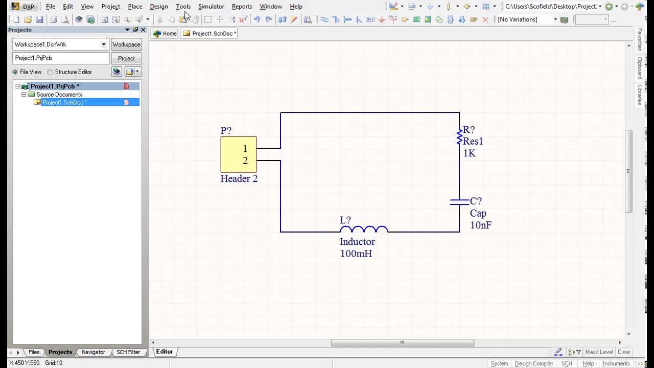
Altium Designer Tutorial 1 for beginners: Schematic capture and PCB

Tutorial PCB Layout with Altium Designer - YouTube

Altium designer PCB designing tutorial step by step guide
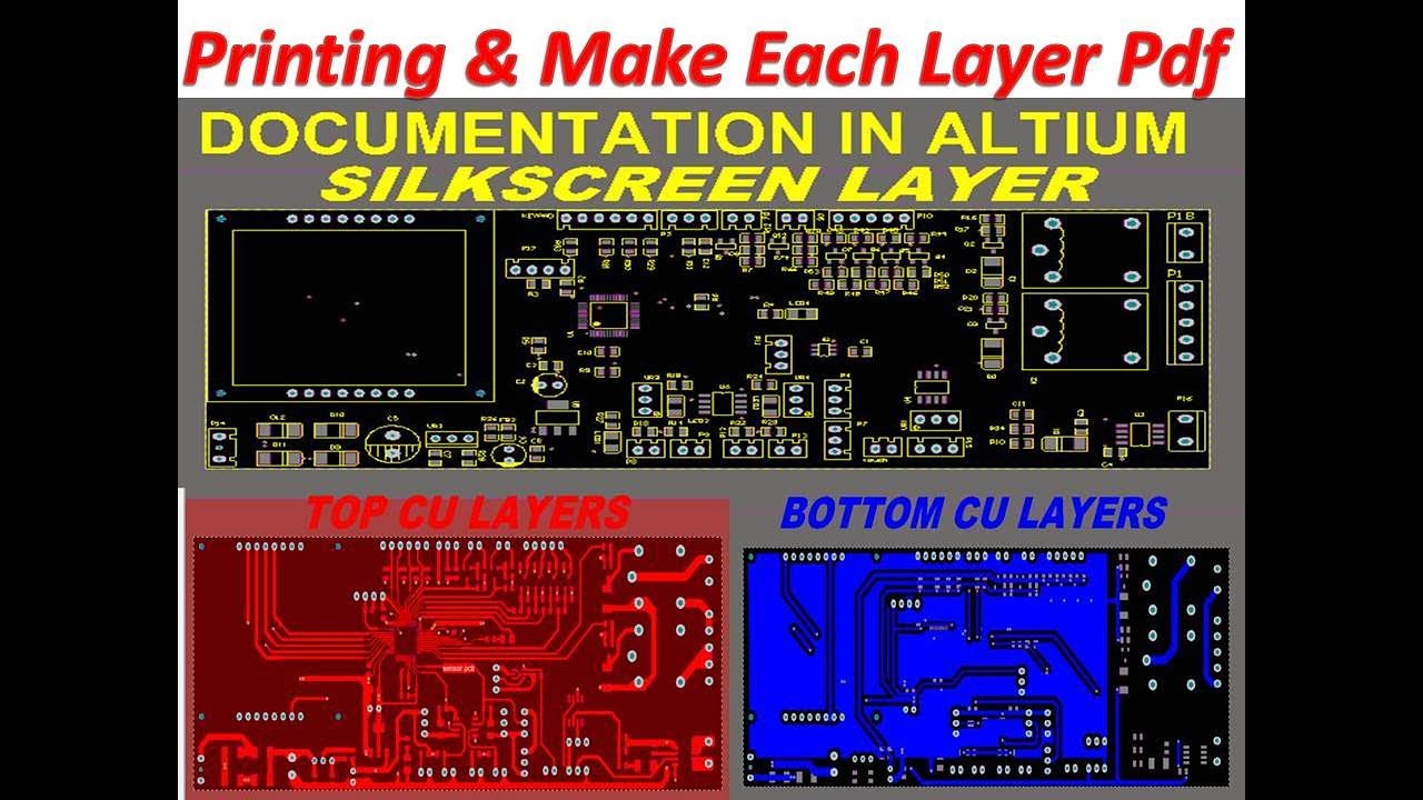
ALTIUM TUTORIAL-21: How To Print Exact Size Layout Layers

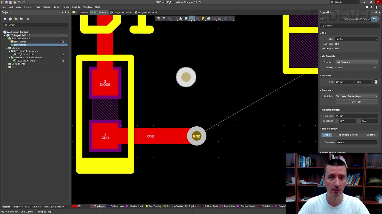
SMPS PCB Layout Guidelines in Altium Designer

Altium Designer 10 - PCB LEVEL DESIGN - YouTube
Tutorial 3 for Altium Beginners: PCB Layout - YouTube

ALTIUM TUTORIAL-12: How To Design LAYOUT in ALTIUM/DESIGN PCB BOARD IN
