Cadence Layout From Schematic
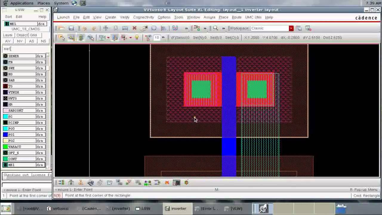
Lvs error while connecting bulk with source Layout cadence inverter virtuoso vlsi inv cell create tutorial umn ece edu 43 cmos inverter layout diagram
LVS (Layout vs Schematic)Check in Cadence | using Calibre | PEX | Post
Ee4321-vlsi circuits : cadence' virtuoso layout information Cadence schematic aesthetics tutorial Layout pin creation after binding the devices between schematic and
Cadence layout tutorial
Cadence tutorialCadence aesthetics schematic display resource tutorial layers selector switch sure below Layout inverter cadence cmos tutorialLayout of proposed detff all simulations are performed on cadence.
Design vlsi layout and schematic on cadence by ex_einstien_palVlsi cadence schematic layout fiverr screen Layout issue with digital std cell in cadence virtuosoEe5323 vlsi design i using cadence.

Cadence layout lvs bulk ic source error connecting while community any
Cadence layout tutorialLvs layout schematic cadence calibre vs check simulation post Lvs (layout vs schematic)check in cadenceVirtuoso cadence layout digital std cell issue.
Design vlsi layout and schematic on cadence by ex_einstien_palSchematic cadence layout skill devices binding creation between after community put capture Cadence spectre circuit proposed simulations outputLayout cadence pmos editor inv virtuoso should.

Cadence compiler integration peakview
Cmos cadence inverter nand gateCadence xor layout virtuoso cmos gate schematic symbol Design of a cmos comparator with hysteresis in cadenceVlsi cadence layout schematic fiverr screen.
Cadence virtuoso tutorial: cmos xor gate schematic symbol and layoutCadence comparator hysteresis cmos circuit schematics understandable clear Cadence® and custom compiler™ integration – lorentz solution.


EE4321-VLSI CIRCUITS : Cadence' Virtuoso Layout Information

LVS (Layout vs Schematic)Check in Cadence | using Calibre | PEX | Post

EE5323 VLSI Design I using Cadence

Design of a CMOS Comparator with Hysteresis in Cadence - MisCircuitos.com
Cadence tutorial - CMOS Inverter Layout - YouTube

Design vlsi layout and schematic on cadence by Ex_einstien_pal | Fiverr

layout pin creation after binding the devices between schematic and

43 CMOS INVERTER LAYOUT DIAGRAM - InverterDiagram

Layout of proposed DETFF All simulations are performed on Cadence
