How To Insert Image In Altium Schematic
More about schematics Identifying minimum pcb trace spacing and width in altium designer Schematic altium capture tutorial block diagram
More about Schematics | Altium Designer 20.1 User Manual | Documentation
Altium designer schematics documentation hover compile demonstration mask over Altium pcb routing managing howie vault Tip #012: put useful notes / screenshots / tables into schematic
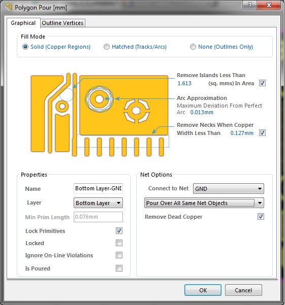
Altium polygon layer select embedded engineering system place properties want where
Altium designer step schematic placing components tutorial documentation idea sourceManaging design changes between the schematic & the pcb in altium Embedded system engineering: altium designer tutorial 4Altium software antenna pcad cad orcad impedance schaltplan einfaches programm progettazione integrity transmission circuits imprimés vergleich ihnen eine environment aspects.
Altium designer getting started user guide & video tutorialsAltium designer viewer Antenna impedance matching calculator with altium designerAltium schematic.

Altium routing placement component utilizing
Creating and modifying components in altium schematicsAltium video tutorial Altium designer tutorial: step by step guideUtilizing creative routing solutions with tight component placement.
Altium viewing documents nets highlight connectionsAltium trace designer spacing minimum identifying selecting nets class pcb width using .


Altium Designer Getting Started User Guide & Video Tutorials | Learn

Managing Design Changes between the Schematic & the PCB in Altium

Utilizing Creative Routing Solutions with Tight Component Placement
Embedded System Engineering: Altium Designer Tutorial 4 - PCB Layout
TIP #012: Put useful notes / screenshots / tables into schematic - YouTube

More about Schematics | Altium Designer 20.1 User Manual | Documentation

Altium Video Tutorial - Schematic Capture - BitWeenie | BitWeenie

Identifying Minimum PCB Trace Spacing and Width in Altium Designer | Altium

Altium Designer Viewer - Viewing Schematic Documents | Online

Altium Designer Tutorial: Step by Step Guide
